    import numpy as np
import plotly.graph_objs as go
from matplotlib import pyplot as plt
from math import pi
Tight binding and nearly free electrons
(based on chapter 16 of the book)
Expected prior knowledge
Before the start of this lecture, you should be able to:
- Apply perturbation theory to understand the band structure at crossings
- Derive the dispersion relation for a tight-binding model
- Recall the notion of the Fermi energy
- Calculate the Fermi surface, i.e. through the Fermi wavevector \(k_F\), for two and three-dimensional systems
- Construct the unit cell of a crystal
Learning goals
After this lecture you will be able to:
- examine 1D and 2D band structures and argue if you expect the corresponding material to be an insulator/semiconductor or a conductor.
- describe how the light absorption spectrum of a material relates to its band structure.
Band structure
In nature we see that some materials conduct electricity (conductors), some don't (insulators), and some do under specific circumstances (semiconductors). The motion of electrons is described by the band structure (dispersion relation). So far we have derived the dispersion relation for different types of models, such as the tight-binding model in which the electrons are bound by a strong potential, or when the electrons are perturbed by a small periodic potential as was the case in the NFEM. We have not yet discussed how the band structure affects the electrical properties of a material.
For a material to be a conductor, there should be available electron states at the Fermi level. Otherwise all the states are occupied, and all the currents cancel out.
Suppose we have a band structure of a 1D material similar to the one below:

We see several energy bands that may either be separated by a band gap or overlap.
When the Fermi level lies in the band gap, the material is called a semiconductor (or dielectric or insulator). When the Fermi level lies within a band, it is a conductor (metal).
Suppose the Fermi energy lies in the band gap. What feature about the band gap determines if a material is insulating or a semiconductor?
Its size
A simple requirement for insulators
In an insulator every single band is either completely filled or completely empty.
What determines if an energy band is fully occupied or only partially occupied? To answer this we need to know the number of available states within an energy band, and the number of electrons in the system. We can find the number of states in a band by integrating the density of states \(g(E)\), but this is hard. Fortunately, we can easily see how many states there are in an energy band by counting the number of \(k\)-states in the first Brillouin zone.
For a single band:
Here, \(L^3/a^3\) is the number of unit cells in the system, so we see that a single band has room for 2 electrons per unit cell (the factor 2 comes from the spin).
We come to the important rule:
Any material with an odd number of electrons per unit cell is a metal.
If the material has an even number of electrons per unit cell it may be a semiconductor, but only if the bands are not overlapping (see the figure above), or it could be a metal. To illustrate this, let us consider the three elements Si (silicon), Ge (germanium) and Sn (tin). All three of these have 4 valence electrons. Both Si (band gap 1.14 eV) and Ge (band gap 0.67 eV) are semiconductors, while Sn (tin) is a metal.
Why is Sn not a semiconductor but a metal?
It has overlapping energy bands
Fermi surface using a nearly free electron model
In the end, we are also interested in studying the electrical properties, and thus the Fermi surface, in higher dimensions as well. One could either do this through a tight-binding model approach (which is very similar to the 1D case), or through the NFEM (same procedure as in 1D, but harder because of the need to imagine a higher dispersion relation). Let us illustrate the procedure in 2D. To derive the corresponding Fermi surface using the NFEM we use the sequence of steps:
- Compute \(k_F\) using the free electron model (remember this is our starting point).
- Plot the free electron model Fermi surface and the Brillouin zones.
- Apply the perturbation where the Fermi surface crosses the Brillouin zone (due to avoided level crossings).
By doing so, the resulting band structure looks like the following (in the extended Brillouin zone scheme):
def E(k_x, k_y):
    delta = np.array([-2*pi, 0, 2*pi])
    H = np.diag(
        ((k_x + delta)[:, np.newaxis]**2
        + (k_y + delta)[np.newaxis]**2).flatten()
    )
    return tuple(np.linalg.eigvalsh(H + 5)[:3])

E = np.vectorize(E, otypes=(float, float, float))

momenta = np.linspace(-2*pi, 2*pi, 100)
kx, ky = momenta[:, np.newaxis], momenta[np.newaxis, :]
bands = E(kx, ky)

# Extended Brillouin zone scheme
pad = .3
first_BZ = ((abs(kx) < pi + pad) & (abs(ky) < pi + pad))
second_BZ = (
    ((abs(kx) > pi - pad) | (abs(ky) > pi - pad))
    & ((abs(kx + ky) < 2*pi + pad) & (abs(kx - ky) < 2*pi + pad))
)
third_BZ = (
    (abs(kx + ky) > 2*pi - pad) | (abs(kx - ky) > 2*pi - pad)
)

bands[0][~first_BZ] = np.nan
bands[1][~second_BZ] = np.nan
#bands[2][~third_BZ] = np.nan

# Actually plotting

go.Figure(
    data = [
        go.Surface(
            z=band / 5,
            # colorscale=color,
            opacity=opacity,
            showscale=False,
            hoverinfo='none',
            colorscale='Reds',
            x=momenta,
            y=momenta,
        )
        for band, opacity
        in zip(bands[:2],
               # ['#cf483d', '#3d88cf'],
               (1, 0.9))
    ],
    layout = go.Layout(
        title='Nearly free electrons in 2D',
        autosize=True,
        hovermode=False,
        margin=dict(
            t=50,
            l=20,
            r=20,
            b=50,
        ),
        scene=dict(
            yaxis={"title": "k_y"},
            xaxis={"title": "k_x"},
            zaxis={"title": "E"},
        )
    )
)
Observe that the top of the first band is above the bottom of the second band. Therefore if \(V\) is sufficiently weak, the material can be conducting even with 2 electrons per unit cell!
A larger \(V\) makes the Fermi surface more distorted and eventually makes the material insulating. Let's compare the almost parabolic dispersion of the nearly free electron model with a tight-binding model in 2D.
For a tight-binding model we obtain the dispersion \(E = E_0 - 2t(\cos k_x a + \cos k_y a)\):
momenta = np.linspace(-pi, pi, 100)
kx, ky = momenta[:, np.newaxis], momenta[np.newaxis, :]
energies = -np.cos(kx) - np.cos(ky)
go.Figure(
    data = [
        go.Surface(
            z=energies,
            # colorscale='#3d88cf',
            opacity=1,
            showscale=False,
            hoverinfo='none',
            x=momenta,
            y=momenta,
        )
    ],
    layout = go.Layout(
        title='Tight-binding in 2D',
        autosize=True,
        hovermode=False,
        margin=dict(
            t=50,
            l=20,
            r=20,
            b=50,
        ),
        scene=dict(
            yaxis={"title": "k_y"},
            xaxis={"title": "k_x"},
            zaxis={"title": "E"},
        )
    )
)
Light absorption
So far we have only discussed the effect of the Fermi energy and the band structure on the electrical properties of a material. We know from nature that photons of external light sources can be reflected, transmitted, or absorbed by a material. Absorption requires energy transfer from the photon to electrons. In a filled band there are no available states where energy could be transferred (that's why insulators may be transparent).
When a transition between two bands becomes possible because the photons have sufficiently high energy, the absorption increases in a step-like fashion. See the sketch below for germanium.

Here \(E'_G\approx 0.9\,\mathrm{eV}\) and \(E_G\approx 0.8\,\mathrm{eV}\). The two visible steps are due to the special band structure of Ge:

This band structure has two band gaps: the direct band gap \(E'_G\) at \(k=0\), and the indirect band gap \(E_G\) between different \(k\)-points. In Ge \(E_G < E'_G\), and therefore it is an indirect band gap semiconductor. Silicon also has an indirect band gap. Direct band gap materials are for example GaAs and InAs.
Photons carry very little momentum for a given energy because \(E = \hbar c k\) and \(c\) is large. Therefore, although a photon with energy \(E_G\) would be sufficient energetically, there is not enough momentum to excite an electron across an indirect band gap. Then an extra phonon is required. Phonons may have a very large momentum at room temperature, and a very low energy since atomic mass is much higher than electron mass.
A joint absorption of a photon and a phonon may excite an electron across an indirect band gap. However, this process is much less efficient, and therefore materials with an indirect band gap are much worse for optical applications (light-emitting diodes, light sensors, etc.).
Summary
- Each band can host two electrons per unit cell, therefore a material with an odd number of electrons per unit cell is a metal; a material with an even number may be an insulator.
- Light absorption is a tool to measure the band gap, and it distinguishes direct from indirect band gaps.
Exercises
Exercise 1: 3D Fermi surfaces
Using the periodic table of the Fermi surfaces, answer the following questions:
- Find 4 elements that are well described by the nearly-free electron model and 4 that are poorly described by it.
- Is the Fermi surface of lithium better described by the free electron model or the NFEM? What about potassium? Why?
- Do you expect a crystal with a simple cubic lattice and monovalent atoms to be conducting?
- Na has 1 valence electron and Cl has 7. What Fermi surface shape would you expect the NaCl crystal to have? Explain your answer using a. the atomic valences, and b. the optical properties of this crystal.
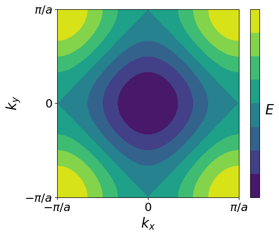
Exercise 2: Tight-binding in 2D
Consider a rectangular lattice with lattice constants \(a_x\) and \(a_y\). Suppose the hopping parameters in the two corresponding directions to be \(-t_1\) and \(-t_2\). We limit ourselves to a single orbital per atom and only nearest-neighbour interactions.
- Write down a 2D tight-binding Schrödinger equation (use your result of 1D).
- Formulate the Bloch ansatz for the wave function.
- Calculate the dispersion relation of this model.
-
The dispersion is plotted below.
What Fermi surface shape would this model have if the atoms are monovalent?
-
What Fermi surface shape would it have if the number of electrons per atom is much smaller than 1?
    def dispersion2D(N=100, kmax=pi, e0=2):

        # Define matrices with wavevector values
        kx = np.tile(np.linspace(-kmax, kmax, N),(N,1))
        ky = np.transpose(kx)

        # Plot dispersion
        plt.figure(figsize=(6,5))
        plt.contourf(kx, ky, e0-np.cos(kx)-np.cos(ky))

        # Making things look ok
        cbar = plt.colorbar(ticks=[])
        cbar.set_label('$E$', fontsize=20, rotation=0, labelpad=15)
        plt.xlabel('$k_x$', fontsize=20)
        plt.ylabel('$k_y$', fontsize=20)
        plt.xticks((-pi, 0 , pi),('$-\pi/a$','$0$','$\pi/a$'), fontsize=17)
        plt.yticks((-pi, 0 , pi),('$-\pi/a$','$0$','$\pi/a$'), fontsize=17)

    dispersion2D()
Exercise 3: Nearly-free electron model in 2D
(based on exercise 15.4 of the book)
Suppose we have a square lattice with lattice constant \(a\), with a periodic potential given by \(V(x,y)=2V_{10}(\cos(2\pi x/a)+\cos(2\pi y/a))+4V_{11}\cos(2 \pi x/a)\cos(2 \pi y/a)\).
-
Use the nearly-free electron model to find the energy of state \(\mathbf{q}=(\pi/a, 0)\).
Hint
This is analogous to the 1D case: the states that interact have \(k\)-vectors \((\pi/a,0)\) and \((-\pi/a,0)\); (\(\psi_{+}\sim e^{i\pi x /a}\) ; \(\psi_{-}\sim e^{-i\pi x /a}\)).
-
Let's now study the more complicated case of state \(\mathbf{q}=(\pi/a,\pi/a)\). How many \(k\)-points have the same energy? Which ones?
- Write down the nearly free electron model Hamiltonian near this point.
-
Find its eigenvalues.
Hint
Make use of the symmetries of the matrix Hamiltonian